| |


Actually the "original" Radar Scope schematics you can see here as PDF (3.3 MB) are of very bad quality. It seems this is not due to bad scans but to the quality of the schematics as they were published around 1980. I learned this the hard way since i bought original manuals from a shop in the US, only to see that they were as lousy as the pdf above. But if you want to do some serious troubleshooting with a Radar Scope boardset you need them all the same. I will make references to them below, and with the aid of a magnifying glass you might even decipher them.
If you have any better ones or want to help redrawing the existing ones please mail me. I am working on this but so far i can only provide a line buffer schematic, you can download it on the video page.
It is very helpful to have a known good video signal source to be able to check a monitor.
You do not need expensive equipment to do this. I use a Tetris bootleg board that has a JAMMA
connector. See here for JAMMA pinout.
These Tetris boards have a little switch. When on, it will boot in setup mode. After 6 presses of the
1P BTN2 (Jamma Pin 23 Component side, connect button to GND) you will have a color test pattern.
But how to connect this to an original TRS-14C color monitor? Since the Nintendo Monitor expects inverted video you have to invert
the RGB Signals using a video inverter circuit. I built one myself but there are also commercial units to be had.
In the end this monitor test setup works for me:

|
The following descriptions are for the attract mode of Radar Scope. It shows
after booting. This is not a stable state, since there are several parts of
the attract mode cycling and repeating (demo, title screen, high score screen),
but these measurements on a working game give a good overview on what states
should be seen or not:
For testing purposes it is very convenient to have a running boardset in a defined state. Because i wanted to exercise my signature analyzer and get some signatures i used a Z80 hardwired to do NOP instructions.
Use 8 resistors 470 Ohms, bend up the Z80 pins number 7,8,9,10,12,13,14,15 and solder the resistors to these pins. The other end of the resistors is soldered to a common wire which you connect to pin 29 (GND). Then bend up Z80 pins 16 (INT), 17 (NMI) and 25 (BUSREQ) and solder 3 pull-up resistors 5.6K to these. The other end of the resistors is soldered to a common wire which you connect to pin 11 (+ 5 Volts) like this:
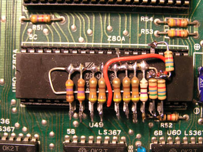
When you insert this Z80 into the socket, data bus pins D0 to D7 are all pulled low, which results in a NOP instruction. The Z80 will loop through the entire address range 0000 to ffff endlessly doing NOP's. The external bus request and the interrupts are disabled.
If you want to know how signature analysis works please read the How Atari Signature Analysis Works. The following signatures were taken with a HP 5004A signature analyzer and the NOP fixture described above.
| PROBE | CONNECT TO | SETTING |
| clock | pin 21 (/rd) | rising edge |
| start/stop | pin 5 (a15) | falling edge |
| ground | tp 1 | - |
| DATA PROBE | PIN | SIGNATURE |
| A0 | 30 | UUUU |
| A1 | 31 | 5555 |
| A2 | 32 | CCCC |
| A3 | 33 | 7F7F |
| A4 | 34 | 5H21 |
| A5 | 35 | 0AFA |
| A6 | 36 | UPFH |
| A7 | 37 | 52F8 |
| A8 | 38 | HC89 |
| A9 | 39 | UNSTABLE? |
| A10 | 40 | HPP0 |
| A11 | 1 | UNSTABLE? |
| A12 | 2 | HAP7 |
| A13 | 3 | 3C96 |
| A14 | 4 | 3827 |
| A15 | 5 | 755U |
| PROBE | CONNECT TO | SETTING |
| clock | 4H, pin 6 (/RFSH input to address decoder 4H) | falling edge |
| start | 4H, pin 15 (/CE chip enable of 5F ROM) | falling edge |
| stop | 4H, pin 15 (/CE chip enable of 5F ROM) | rising edge |
| ground | TP 1 | - |
| DATA PROBE | PIN | SIGNATURE |
| D0 | 9 | 5HF7 |
| D1 | 10 | 8P65 |
| D2 | 11 | FA26 |
| D3 | 13 | 4P20 |
| D4 | 14 | C113 |
| D5 | 15 | 4C52 |
| D6 | 16 | 332P |
| D7 | 17 | P418 |
| PROBE | CONNECT TO | SETTING |
| clock | 4H, pin 6 (/RFSH input to address decoder 4H) | falling edge |
| start | 4H, pin 14 (/CE chip enable of 5G ROM) | falling edge |
| stop | 4H, pin 14 (/CE chip enable of 5G ROM) | rising edge |
| ground | TP 1 | - |
| DATA PROBE | PIN | SIGNATURE |
| D0 | 9 | A5PC |
| D1 | 10 | 026U |
| D2 | 11 | C53F |
| D3 | 13 | 3575 |
| D4 | 14 | 8A40 |
| D5 | 15 | 899H |
| D6 | 16 | 6H90 |
| D7 | 17 | 149F |
| PROBE | CONNECT TO | SETTING |
| clock | 4H, pin 6 (/RFSH input to address decoder 4H) | falling edge |
| start | 4H, pin 13 (/CE chip enable of 5H ROM) | falling edge |
| stop | 4H, pin 13 (/CE chip enable of 5H ROM) | rising edge |
| ground | TP 1 | - |
| DATA PROBE | PIN | SIGNATURE |
| D0 | 9 | P10C |
| D1 | 10 | PC07 |
| D2 | 11 | H5HC |
| D3 | 13 | 6634 |
| D4 | 14 | A0P3 |
| D5 | 15 | 213P |
| D6 | 16 | 6UP3 |
| D7 | 17 | 6P7H |
| PROBE | CONNECT TO | SETTING |
| clock | 4H, pin 6 (/RFSH input to address decoder 4H) | falling edge |
| start | 4H, pin 12 (/CE chip enable of 5K ROM) | falling edge |
| stop | 4H, pin 12 (/CE chip enable of 5K ROM) | rising edge |
| ground | TP 1 | - |
| DATA PROBE | PIN | SIGNATURE |
| D0 | 9 | 8HFU |
| D1 | 10 | 1AFA |
| D2 | 11 | 2550 |
| D3 | 13 | 19U0 |
| D4 | 14 | 9AA5 |
| D5 | 15 | H6AC |
| D6 | 16 | 96F3 |
| D7 | 17 | 446F |
On a TRS2-04-SOU board described here only the MB8516 EPROM at Pos.
3I is present for the sound samples.
The SOU board controller is an Intel 8035. It sends the sample data to a digital-to-analog converter DAC-08.
You can test the SOU board using the NOP fixture shown above.
By connecting the board to power you can trigger the different sounds shown on my SOU page.
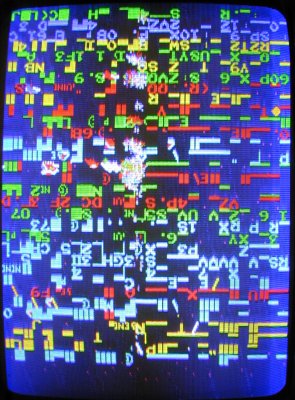
| On power up there is a static
screen as shown below.
Sound is not present. The left screen side is filled with random upside
down characters. The blue background (which is hardware generated) is
present.
Sprites or parts of sprites can be seen. The game does not react to coin switch or service button. 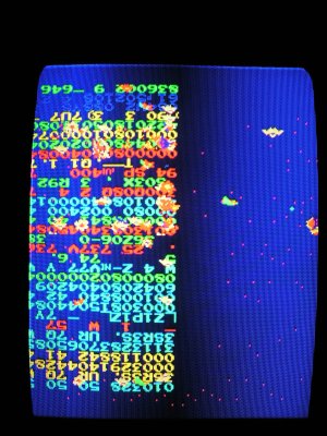 |
troubleshooting: The CPU board is folded out of the casing, logic tester connected to TP1 (GND) and +5V (right side of capacitor C24 near power plug P8). checking reset: At Pos. 3L (7404, Pin 4) LOW directy after power up, then permanently HIGH. Also TP8 RESET signal stays HIGH and the same at Z80 CPU, pin 26. The reset signal appears to be OK. checking Z80 CPU: Pin 5 (address line A15) pulses with approx. 2 Hz Pin 17 (NMI) sticks HIGH. This is in contrast to the normal state described above, because NMI should go LOW with VBLK (vertical blanking). Pin 23 BUSAK and Pin 25 BUSRQ are constantly HIGH, there are no DMA transfers taking place. checking 8257 DMA Controller: Pin 3 MEMR and Pin 4 MEMW are stuck HIGH. No DMA transfer is possible. checking EPROMS: All Chip Enable signals at the EPROMS (each pin 20) are present. checking RAM: All Chip Select signals at the RAMs (each Pin 8) of 6H, 6L, 6J, 6M, 6K, 6N are HIGH. The RAM must be blocked somehow. Since there are no CS signals for RAM, the address decoding is examined: The 74LS138 address decoder at position 4K which decodes the RAMs must be enabled by appropriate signals at pins 4, 5 and 6. Since pin 4 is stuck HIGH, the chip will never be enabled. The logic probe on the NOR gate going to this pin shows both missing /RD and /WR signals. These signals go out from the CPU at pin 21 (/RD) and pin 22 (/WR) then are buffered at a buffer (74LS367) at Pos. 6B. On the input side of this buffer both signals are present, while they disappear at the appropriate output pins. After replacing this buffer |
In this state it is possible to
give service credits and to start the
game. The left side of the screen looks normal, while the right side is
partially garbled with characters. There is no sound.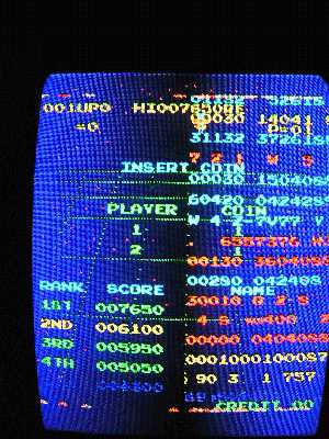 |
This time the remaining buffers (74LS367) are also
checked to make sure if still another bus signal ist faulty. At Pos. 6A
there is another 74367 which shows a signal at pin 10 (input)
but no defined level at the output (pin 9). This was the outgoing A0
address line to the video board. Since this time only memory access to the video / text ROMS was disturbed, the game could boot and work to a certain extent. After replacing this buffer chip the game was working as it should. Note: The probable cause of these two chips failing was accumulated (and moist) dust, since positions 6A and 6B are just at the edge of the PCB, the spot where the cooling fan in the cabinet is positioned. After several years of operation, accumulated dust began to cake between the IC pins and the parts failed. |
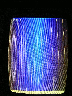 |
Visible retrace lines while the stars background is still there. (The moiré pattern here is due to my bad picture, not the fault itself.) This can be symptom of a bad connection on the ESS board (check connector P5) of a TRS01 boardset variant. |
 |
This is a freezing of the game before it can get to the attract mode, possibly caused by defective ram |
 |
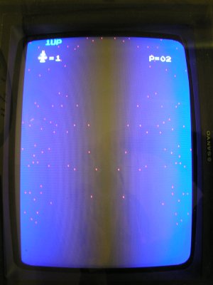
This picture shows a game where the cpu executes NOP's endlessly. Note that the blue to black to blue background and the stars are there! The background and the stars are hardware generated by the video board and not done by software. So this screen should not lead you to believe that the CPU is working at all. The screen shows a (slightly flickering) image of background with an overlay of text screen with random characters. This is the random content of the background video RAM, which has not been initialized (cleared) by the software. |
 |
 |
| The sprite (here the gun) has missing vertical lines | This is how it should look like |
 |
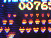 |
| All objects have the same defects | This is how it should look like |
What looks like a problem with vertical lines is actually a horizontal problem: The missing lines are due to a defective line buffer. This line buffer is a buffer for a complete horizontal line.
If this seems strange, consider the fact that Radar Scope is just vertically oriented: The top down lines are actually the horizontal raster! (See note on the video page) But why are the background graphics unaffected? This is because the two line buffers in Radar Scope are used for the sprites (or foreground objects) only. The static background objects (text or graphics) are mixed in by a multiplexer just before the output stage.
Read more about the video display system on the video page. In this particular case the first (of two) line buffers was defective. Both line buffers are on the CLK board. Each is built with two Fujitsu MB7072 ECL RAM's (256 x 4 bit). Buffer 1 is at position 5L and 5M and buffer 2 at 5N and 5P. Since a horizontal line is 256 pixels wide and the sprite data is 6 bits per pixel, 256 x 6 bits are needed. Two MB7072 RAM's in parallel provide 256 x 8 bits. On each RAM, one bit Input / Output is therefore unused.